
TOPIC 5: ELECTRONIC

OTHER TOPICS
Semi Conductors
The Concept of Energy Band in Solids
Explain the concept of energy bands in solids
In solid-state physics, the electronic band structure (or simply band structure) of a solid describes those ranges of energy that an electron within the solid may have (called energy bands, allowed bands, or simply bands) and ranges of energy that it may not have (called band gaps or forbidden bands).
Band theory derives these bands and band gaps by examining the allowed quantum mechanical wave functions for an electron in a large, periodic lattice of atoms or molecules. Band theory has been successfully used to explain many physical properties of solids, such as electrical resistivity and optical absorption, and forms the foundation of the understanding of all solid-state devices (transistors, solar cells, etc.).
Difference between Conductors, Semiconductors and Insulators
Distinguish between conductors, semiconductors and insulators
Insulators
An electrical insulator is a material whose internal electric charges do not flow freely, and therefore make it impossible to conduct an electric current under the influence of an electric field. This contrasts with other materials, semiconductors and conductors, which conduct electric current more easily.
The property that distinguishes an insulator is its resistivity; insulators have higher resistivity than semiconductors or conductors.
A perfect insulator does not exist, because even insulators contain small numbers of mobile charges (charge carriers) which can carry current. In addition, all insulators become electrically conductive when a sufficiently large voltage is applied that the electric field tears electrons away from the atoms. This is known as the breakdown voltage of an insulator.
Some materials such as glass, paper and Teflon, which have high resistivity, are very good electrical insulators. A much larger class of materials, even though they may have lower bulk resistivity, are still good enough to prevent significant current from flowing at normally used voltages, and thus are employed as insulation for electrical wiring and cables. Examples include rubber-like polymers and most plastics.
Conductors
A conductor is an object or type of material that allows the flow of electrical current in one or more directions. For example, a wire is an electrical conductor that can carry electricity along its length.
In metals such as copper or aluminum, the movable charged particles are electrons. Positive charges may also be mobile, such as the cationic electrolyte(s) of a battery, or the mobile protons of the proton conductor of a fuel cell. Insulators are non-conducting materials with few mobile charges and support only insignificant electric currents.
Semiconductors
A semiconductor material has an electrical conductivity value falling between that of a conductor, such as copper, and an insulator, such as glass. Semiconductors are the foundation of modern electronics. Semiconducting materials exist in two types: elemental materials andcompound materials.
The modern understanding of the properties of a semiconductor relies on quantum physics to explain the movement of electrons and holes in a crystal lattice. The unique arrangement of the crystal lattice makes silicon and germanium the most commonly used elements in the preparation of semiconducting materials.
An increased knowledge of semiconductor materials and fabrication processes has made possible continuing increases in the complexity and speed of microprocessors and memory devices. Some of the information on this page may be outdated within a year because new discoveries are made in the field frequently.
Examples of semiconductors are Silicon, Germanium.
The Effects of Temperature on the Conductivity of Conductors, Semiconductors and Insulators
Describe the effect of temperature on the conductivity of conductors, semiconductors and insulators
The conductivity of pure defect free metal decreases with increase in temperature .With increased temperature in a metal, thermal energy causes atoms in metal to vibrate, in this excited state atoms interact with and scatter electrons.
Thus decreasing the mean free path, and hence the mobility of electrons too decreases, and resistivity increases.
Since, resistivity = 1/conductivity
The electrical conductivity of a semiconductor will increase exponentially with an increase in temperature, as temperature increases the electrons in the valance band will gain energy and go into the higher energy levels in the conduction band where they become charge carriers.
The increase in conduction can also be explained, I guess,due to the formation of Cooper pairs and hence the creation of Phonon field.
Types of Semiconductors
Identify types of Semiconductors
There are two types of semiconductors
- Intrinsic semiconductors
- Extrinsic semiconductors
Intrinsic semiconductors
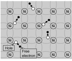
An intrinsic semiconductor material is chemically very pure and possesses poor conductivity. It has equal numbers of negative carriers (electrons) and positive carriers (holes). Examples are Silicon and Germanium.
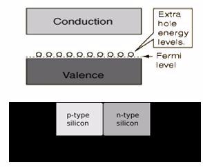
A silicon crystal is different from an insulator because at any temperature above absolute zero temperature, there is a finite probability that an electron in the lattice will be knocked loose from its position, leaving behind an electron deficiency called a "hole."
If a voltage is applied, then both the electron and the hole can contribute to a small current flow.The conductivity of a semiconductor can be modeled in terms of the band theory of solids.
The band model of a semiconductor suggests that at ordinary temperatures there is a finite possibility thatelectrons can reach the conduction band and contribute to electrical conduction. The term intrinsic heredistinguishes between the properties of pure "intrinsic" silicon and the dramatically different properties ofdoped n-type or p-type semiconductors.
The current flow in an intrinsic semiconductor is influenced by the density of energy states which in turn influencesthe electron density in the conduction band. This current is highly temperature dependent. The electrical conductivityof intrinsic semiconductors increase with increasing temperature.
Extrinsic semiconductors
Extrinsic semiconductor is an improved intrinsic semiconductor with a small amount of impurities added by a process,known as doping, which alters the electrical properties of the semiconductor and improves its conductivity.
Introducing impurities into the semiconductor materials (doping process) can control their conductivity.Doping process produces two groups of semiconductors:
- The negative charge conductor (n-type).
- The positive charge conductor (p-type).
Semiconductors are available as either elements or compounds. Silicon and Germanium are the most commonelemental semiconductors. Compound Semiconductors include InSb, InAs, GaP, GaSb, GaAs, SiC, GaN. Si and Geboth have a crystalline structure called the diamond lattice. That is, each atom has its four nearestneighbors at the corners of a regular tetrahedron with the atom itself being at the center.
In addition to the pure element semiconductors, many alloys and compounds are semiconductors.The advantage of compound semiconductor is that they provide the device engineer with a wide range of energy gapsand mobilities, so that materials are available with properties that meet specific requirements. Some of thesesemiconductors are therefore called wide band gap semiconductors.
The Mechanism of Doping Intrinsic Semiconductors
Describe the mechanism of doping intrinsic semiconductors
The addition of a small percentage of foreign atoms in the regular crystal lattice of silicon or germanium produces dramatic changes in their electrical properties, producing n-type and p-type semiconductors.
Pentavalent impurities
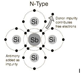
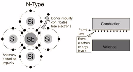
The addition of pentavalent impurities such as antimony,arsenic or phosphorous contributes free electrons, greatly increasing the conductivity of the intrinsic semiconductor. Phosphorous may be added by diffusion of phosphine gas (PH3).(5 valence electrons) produce n-type semiconductors by contributing extra electrons.
Trivalent impurities
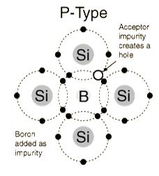
(3 valence electrons) produce p-type semiconductors by producing a "hole" or electron deficiency.
N-Type Semiconductor
The addition of pentavalent impurities such as antimony, arsenic or phosphorous contributes free electrons,greatly increasing the conductivity of the intrinsic semiconductor. Phosphorous may be added by diffusion ofphosphine gas (PH3).
P-Type Semiconductor
The addition of trivalent impurities such as boron, aluminum or gallium to an intrinsic semiconductor creates deficiencies of valence electrons,called "holes". It is typical to use B2H6diborane gas to diffuse boron into the silicon material.
P-n junctions
P-n junctions are formed by joining n-type and p-type semiconductor materials.
Since the n-type region has a high electron concentration and the p type a high hole concentration, electrons diffuse from the n-type side to the p-type side. Similarly, holes flow by diffusion from the p-type side to the n-type side.
If the electrons and holes were not charged, this diffusion process would continue until the concentration of electrons and holes on the two sides were the same, as happens if two gasses come into contact with each other. However, in a p-n junction, when the electrons and holes move to the other side of the junction, they leave behind exposed charges on dopant atom sites, which are fixed in the crystal lattice and are unable to move.
On the n-type side, positive ion cores are exposed. On the p-type side, negative ion cores are exposed. An electric field Ê forms between the positive ion cores in the n-type material and negative ion cores in the p-type material. This region is called the "depletion region" since the electric field quickly sweeps free carriers out, hence the region is depleted of free carriers.
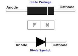
Diodes
A semiconductor diode is a crystalline piece of semiconductor material with a p–n junction connected to two electrical terminals.In electronics, a diode is a two-terminal electronic component with asymmetric conductance; it has low (ideally zero) resistance to current in one direction, and high (ideally infinite) resistance in the other
The Construction of P-N Junction
Describe the construction of P-N junction
When the polarity of the battery is such that electrons are allowed to flow through the diode, the diode is said to be forward-biased. Conversely, when the battery is “backward” and the diode blocks current, the diode is said to be reverse-biased. A diode may be thought of as like a switch: “closed” when forward-biased and “open” when reverse-biased.
Diode behavior is analogous to the behavior of a hydraulic device called a check valve. A check valve allows fluid flow through it in only one direction.
The Mode of Action a P-N Junction
Explain the mode of action of a P-N junction
In a p-n junction, electrons cross over the boundary from the n-type material to holes in the p-type material. At the same time, holes cross over from the p-side to the n-side and capture electrons. This movement of holes and electrons causes the n-side to become positively charged and the p-side to become negatively charged. A p.d is created across the junction to stop further electron flow.
The Types of Diodes
Identify the types of diodes
There are different types of diodes, the following are the most common ones:
- Backward diode: This type of diode is sometimes also called the back diode. Although not widely used, it is a form of PN junction diode that is very similar to the tunnel diode in its operation. It finds a few specialist applications where its particular properties can be used. Read more about the Backward diode.
- BARITT diode: This form of diode gains its name from the words Barrier Injection Transit Time diode. It is used in microwave applications and bears many similarities to the more widely used IMPATT diode.
- Gunn Diode:Although not a diode in the form of a PN junction, this type of diode is a semiconductor device that has two terminals. It is generally used for generating microwave signals. Gunn diode
- Laser diode:This type of diode is not the same as the ordinary light emitting diode because it produces coherent light. Laser diodes are widely used in many applications from DVD and CD drives to laser light pointers for presentations. Although laser diodes are much cheaper than other forms of laser generator, they are considerably more expensive than LEDs. They also have a limited life.
- Light emitting diodes:The light emitting diode or LED is one of the most popular types of diode. When forward biased with current flowing through the junction, light is produced. The diodes use components miconductors, and can produce a variety of colours, although the original colour was red. There are also very many new LED developments that are changing the way displays can be used and manufactured. High output LEDs and OLEDs are two examples.
- Photodiode:The photo-diode is used for detecting light. It is found that when light strikes a PN junction it can create electrons and holes. Typically photo-diodes are operated under reverse bias conditions where even small amounts of current flow resulting from the light can be easily detected. Photo-diodes can also be used to generate electricity. For some applications, PIN diodes work very well as photodetectors.
- PIN diode:This type of diode is typified by its construction. It has the standard P type and N-type areas, but between them there is an area of Intrinsic semiconductor which has no doping. The area of the intrinsicse miconductor has the effect of increasing the area of the depletion region which can be useful for switching applications as well as for use in photodiodes, etc.
- PN Junction: The standard PN junction may be thought of as the normal or standard type of diode in use today. These diodes can come as small signal types for use in radio frequency, or other low current applications which may be termed as signal diodes. Other types may be intended for high current and high voltage applications and are normally termed rectifier diodes.
- Schottky diodes:This type of diode has a lower forward voltage drop than ordinary silicon PN junction diodes. At low currents the drop may be somewhere between 0.15 and 0.4 volts as opposed to 0.6 volts for a silicon diode. To achieve this performance they are constructed in a different way to normal diodes having a metal to semiconductor contact. They are widely used as clamping diodes, in RF applications, and also for rectifier applications.
- Step recovery diode:A form of microwave diode used for generating and shaping pulses at very high frequencies. These diodes rely on a very fast turn off characteristic of the diode for their operation.
- Tunnel diode:Although not widely used today, the tunnel diode was used for microwave applications where its performance exceeded that of other devices of the day.
- Varactor diode or varicap diode:This type of diode is used in many radio frequency (RF) applications. The diode has a reverse bias placed upon it and this varies the width of the depletion layer according to thevoltage placed across the diode. In this configuration the varactor or varicap diode acts like a capacitor with the depletion region being the insulating dielectric and the capacitor plates formed by the extent of the conduction regions. The capacitance can be varied by changing the bias on the diode as this will vary the width of the depletion region which will accordingly change the capacitance.
- Zener diode:The Zener diode is a very useful type of diode as it provides a stable reference voltage. As a result it is used in vast quantities. It is run under reverse bias conditions and it is found that when a certain voltage is reached it breaks down. If the current is limited through a resistor, it enables a stable voltage to be produced. This type of diode is therefore widely used to provide a reference voltage in power supplies. Two types of reverse breakdown are apparent in these diodes: Zener breakdown and Impact Ionisation. However the name Zener diode is used for the reference diodes regardless of the form of breakdown that is employed.
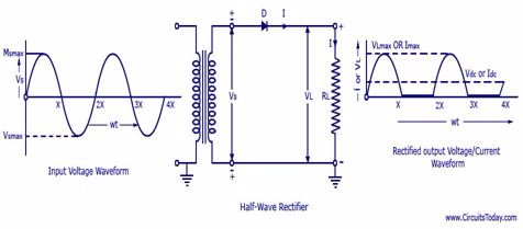
The Construction of a Half-wave and Full-Wave Rectifier
Construct a half-wave and full-Wave rectifier
A rectifier is an electrical device that converts alternating current (AC), which periodically reverses direction,to direct current (DC), which flows in only one direction. The process is known as rectification.
Transistor
The Construction of a PNP Transistor
Describe the construction of a PNP transistor
A transistor is a semiconductor device used to amplify and switch electronic signals and electrical power.It is composed of semiconductor material with at least three terminals for connection to an external circuit.
The Mode of Action of a PNP Transistor
Explain the mode of action of a PNP transistor
The transistor is the fundamental building block of modern electronic devices, and is ubiquitous in modern electronic systems.
A voltage or current applied to one pair of the transistor's terminals changes the current through another pair of terminals. Because the controlled (output) power can be higher than the controlling (input) power, a transistor can amplify a signal.
The Types of Transistors
Identify the types of transistors
There are two types of transistors, which have slight differences in how they are used in a circuit:
- Bipolar transistor
- Field-effect transistor
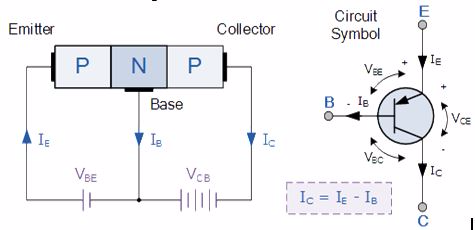
Bipolar transistor
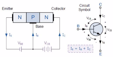
A bipolar transistor has three terminals labeled base, collector, and emitter. A small current at the base terminal (that is, flowing between the base and the emitter) can control or switch a much larger current between the collector and emitter terminals. There are two types of bipolar transistors:
- n-p-n transistors
- p-n-p transistors
Field-effect transistor
For a field-effect transistor, the terminals are labeled gate, source, and drain, and a voltage at the gate can control a current between source and drain.
N-P-N transistor
(Note: Arrow defines the emitter and conventional current flow, “out” for a Bipolar NPN Transistor).
The construction and terminal voltages for a Bipolar NPN Transistor are shown above. The voltage between the Base and Emitter ( VBE ), is positive at the Base and negative at the Emitter because for an NPN transistor, the Base terminal is always positive with respect to the Emitter. Also the Collector supply voltage is positive with respect to the Emitter ( VCE ). So for a bipolar NPN transistor to conduct the Collector is always more positive with respect to both the Base and the Emitter.
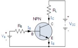
NPN Transistor Connection
Then the voltage sources are connected to an NPN transistor as shown. The Collector is connected to the supply voltage VCC via the load resistor, RL which also acts to limit the maximum current flowing through the device. The Base supply voltage VB is connected to the Base resistor RB, which again is used to limit the maximum Base current.
So in a NPN Transistor it is the movement of negative current carriers (electrons) through the Base region that constitutes transistor action, since these mobile electrons provide the link between the Collector and Emitter circuits. This link between the input and output circuits is the main feature of transistor action because the transistors amplifying properties come from the consequent control which the Base exerts upon the Collector to Emitter current.
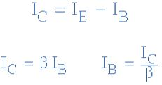
Then we can see that the transistor is a current operated device (Beta model) and that a large current ( Ic ) flows freely through the device between the collector and the emitter terminals when the transistor is switched “fully-ON”. However, this only happens when a small biasing current ( Ib ) is flowing into the base terminal of the transistor at the same time thus allowing the Base to act as a sort of current control input.
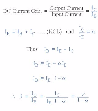
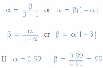
The transistor current in a bipolar NPN transistor is the ratio of these two currents ( Ic/Ib ), called the DC Current Gain of the device and is given the symbol of hfe or nowadays Beta, ( β ). The value of β can be large up to 200 for standard transistors, and it is this large ratio between Ic and Ib that makes the bipolar NPN transistor a useful amplifying device when used in its active region as Ib provides the input and Ic provides the output. Note that Beta has no units as it is a ratio.
Also, the current gain of the transistor from the Collector terminal to the Emitter terminal, Ic/Ie, is called Alpha, ( α ), and is a function of the transistor itself (electrons diffusing across the junction). As the emitter current Ie is the sum of a very small base current plus a very large collector current, the value of alpha α, is very close to unity, and for a typical low-power signal transistor this value ranges from about 0.950 to 0.999.
α and β Relationship in a NPN Transistor
By combining the two parameters α and β we can produce two mathematical expressions that gives the relationship between the different currents flowing in the transistor.
The values of Beta vary from about 20 for high current power transistors to well over 1000 for high frequency low power type bipolar transistors. The value of Beta for most standard NPN transistors can be found in the manufactures data sheets but generally range between 50 – 200.
The equation above for Beta can also be re-arranged to make Ic as the subject, and with a zero base current ( Ib = 0 ) the resultant collector current Ic will also be zero, ( β x 0 ). Also when the base current is high the corresponding collector current will also be high resulting in the base current controlling the collector current. One of the most important properties of the Bipolar Junction Transistor is that a small base current can control a much larger collector current. Consider the following example.
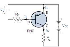
P-N-P transistor
The PNP Transistor is the exact opposite to the NPN Transistor device we looked at in the previous tutorial. Basically, in this type of transistor construction the two diodes are reversed with respect to the NPN type giving a Positive-Negative-Positive type of configuration, with the arrow which also defines the Emitter terminal this time pointing inwards in the transistor symbol.
Also, all the polarities for a PNP transistor are reversed which means that it “sinks” current into its Base as opposed to the NPN Transistor which “sources” current through its Base. The main difference between the two types of transistors is that holes are the more important carriers for PNP transistors, whereas electrons are the important carriers for NPN transistors.
Then, PNP transistors use a small base current and a negative base voltage to control a much larger emitter-collector current. In other words for a PNP transistor, the Emitter is more positive with respect to the Base and also with respect to the Collector.The construction of a “PNP transistor” consists of two P-type semiconductor materials either side of an N-type material as shown below.
(Note: Arrow defines the emitter and conventional current flow, “in” for a PNP transistor).
The construction and terminal voltages for an NPN transistor are shown above. The PNP Transistorhas very similar characteristics to their NPN bipolar cousins, except that the polarities (or biasing) of the current and voltage directions are reversed for any one of the possible three configurations looked at in the first tutorial, Common Base, Common Emitter and Common Collector.
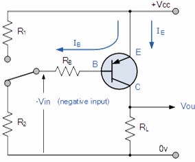
PNP Transistor Connection
The voltage between the Base and Emitter ( VBE ), is now negative at the Base and positive at the Emitter because for a PNP transistor, the Base terminal is always biased negative with respect to the Emitter.Also the Emitter supply voltage is positive with respect to the Collector ( VCE ). So for a PNP transistor to conduct the Emitter is always more positive with respect to both the Base and the Collector.
The voltage sources are connected to a PNP transistor are as shown. This time the Emitter is connected to the supply voltage VCC with the load resistor, RL which limits the maximum current flowing through the device connected to the Collector terminal. The Base voltage VB which is biased negative with respect to the Emitter and is connected to the Base resistor RB, which again is used to limit the maximum Base current.
To cause the Base current to flow in a PNP transistor the Base needs to be more negative than the Emitter (current must leave the base) by approx. 0.7 volts for a silicon device or 0.3 volts for a germanium device with the formulas used to calculate the Base resistor, Base current or Collector current are the same as those used for an equivalent NPN transistor and is given as.
We can see that the fundamental differences between a NPN Transistor and a PNP Transistor is the proper biasing of the transistors junctions as the current directions and voltage polarities are always opposite to each other. So for the circuit above: Ic = Ie – Ib as current must leave the Base.
Generally, the PNP transistor can replace NPN transistors in most electronic circuits, the only difference is the polarities of the voltages, and the directions of the current flow. PNP transistors can also be used as switching devices and an example of a PNP transistor switch is shown below.
The Output Characteristics Curves for a PNP transistor look very similar to those for an equivalent NPN transistor except that they are rotated by 180o to take account of the reverse polarity voltages and currents, (the currents flowing out of the Base and Collector in a PNP transistor are negative). The same dynamic load line can be drawn onto the I-V curves to find the PNP transistors operating points.
The Application of Transistors in Daily Life
Outline the applications of transistors in daily life
Transistors are used in all electronic devices such as calculators, tv, radios, computers etc.
They are used in switching circuits, amplifier circuits, oscillator circuits, current source circuits, voltage regulator circuits, power supply circuits, digital logic intergrated circuits and in any circuit that uses small control signals to control larger currents.
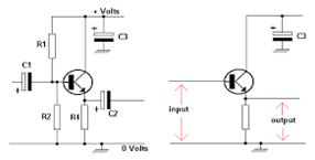
Single Stage Amplifier
The Concept of Analogue Signals
Explain the concept of analogue signals
An Analog signal is any continuous signal for which the time varying feature (variable) of the signal is a representation of some other time varying quantity, i.e., analogous to another time varying signal. It differs from a digital signal in terms of small fluctuations in the signal which are meaningful.
The Concept of Digital Signal
Explain the concept of digital signal
A digital signal uses discrete (discontinuous) values. By contrast, non-digital (or analog) systems use a continuous range of values to represent information. Although digital representations are discrete, the information represented can be either discrete, such as numbers or letters, or continuous, such as sounds, images, and other measurements of continuous systems.
Properties of Digital vs Analog signals
Digital information has certain properties that distinguish it from analog communication methods. These include:
- Synchronisation – digital communication uses specific synchronisation sequences for determining synchronisation.
- Language – digital communications requires a language which should be possessed by both sender and receiver and should specify meaning of symbol sequences.
- Errors – disturbances in analog communication causes errors in actual intended communication but disturbances in digital communication does not cause errors enabling error free communication. Errors should be able to substitute, insert or delete symbols to be expressed.
- Copying – analog communication copies are quality wise not as good as their originals while due to error free digital communication, copies can be made indefinitely.
- Granularity – for a continuously variable analog value to be represented in digital form there occur quantization error which is difference in actual analog value and digital representation and this property of digital communication is known as granularity.
Differences in Usage in Equipment
Many devices come with built in translation facilities from analog to digital. Microphones and speaker are perfect examples of analog devices. Analog technology is cheaper but there is a limitation of size of data that can be transmitted at a given time.
Digital technology has revolutionized the way most of the equipments work. Data is converted into binary code and then reassembled back into original form at reception point. Since these can be easily manipulated, it offers a wider range of options. Digital equipment is more expensive than analog equipment.
Comparison of Analog vs Digital Quality:Digital devices translate and reassemble data and in the process are more prone to loss of quality as compared to analog devices. Computer advancement has enabled use of error detection and error correction techniques to remove disturbances artificially from digital signals and improve quality
Differences in Applications:Digital technology has been most efficient in cellular phone industry. Analog phones have become redundant even though sound clarity and quality was good.
Analog technology comprises of natural signals like human speech. With digital technology this human speech can be saved and stored in a computer. Thus digital technology opens up the horizon for endless possible uses.
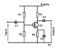
A Single-Stage Amplifier
Design a single-stage amplifier
Single-stage amplifierhave only one amplifying device. It consists of amplification stage that includes a transistor. The transistor is connected to a load resistor through which a load current flows. The value of the load resistor together with the transconductance value affects the amplifier’s voltage gain.
Single-stage amplifiers include:
- Common-emitter (CE) amplifier
- Common-collector (CC) amplifier
- Common-base (CB) amplifier
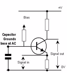
It is called the common-emitter configuration because (ignoring the power supply battery) both the signal source and the load share the emitter lead as a common connection point
Common-emitter amplifier
It is called the common-emitter configuration because (ignoring the power supply battery) both the signal source and the load share the emitter lead as a common connection point
Common-emitter amplifier: The input and output signals both share a connection to the emitter
Before, a small solar cell current saturated a transistor, illuminating a lamp. Knowing now that transistors are able to “throttle” their collector currents according to the amount of base current supplied by an input signal source, we should see that the brightness of the lamp in this circuit is controllable by the solar cell’s light exposure. When there is just a little light shone on the solar cell, the lamp will glow dimly. The lamp’s brightness will steadily increase as more light falls on the solar cell.
Common collector amplifier
It is called the common-collector configuration because (ignoring the power supply battery) both the signal source and the load share the collector lead as a common connection point
Common collector: Input is applied to base and collector. Output is from emitter-collector circuit.
It should be apparent that the load resistor in the common-collector amplifier circuit receives both the base and collector currents, being placed in series with the emitter. Since the emitter lead of a transistor is the one handling the most current (the sum of base and collector currents, since base and collector currents always mesh together to form the emitter current), it would be reasonable to presume that this amplifier will have a very large current gain. This presumption is indeed correct: the current gain for a common-collector amplifier is quite large, larger than any other transistor amplifier configuration. However, this is not necessarily what sets it apart from other amplifier designs.
Common-base amplifier
It is called the common-base configuration because (DC power source aside), the signal source and the load share the base of the transistor as a common connection point shown in.
Common-base amplifier: Input between emitter and base, output between collector and base.
Perhaps the most striking characteristic of this configuration is that the input signal source must carry the full emitter current of the transistor, as indicated by the heavy arrows in the first illustration. As we know, the emitter current is greater than any other current in the transistor, being the sum of base and collector currents. In the last two amplifier configurations, the signal source was connected to the base lead of the transistor, thus handling the least current possible.
Because the input current exceeds all other currents in the circuit, including the output current, the current gain of this amplifier is actually less than 1 (notice how Rload is connected to the collector, thus carrying slightly less current than the signal source). In other words, it attenuates current rather than amplifying it. With common-emitter and common-collector amplifier configurations, the transistor parameter most closely associated with gain was β. In the common-base circuit, we follow another basic transistor parameter: the ratio between collector current and emitter current, which is a fraction always less than 1. This fractional value for any transistor is called the alpha ratio, or α ratio.
OTHER TOPICS
FORM FOUR PHYSICS STUDY NOTES TOPIC 5: ELECTRONIC
4/
5
Oleh
Unknown